|
|
科学研究
|
 |
|
 |
|
学院新闻
|
|
|
|
|
通知公告
|
|
|
|
|
|
|
|
Nano Layer Sacrificial Etching by XeF2(纳米牺牲层刻蚀技术)
科研动态 2013-08-05 15:43 已被浏览 4868 次
通过牺牲层刻蚀技术制备的先进衬底材料
GaAs-on-Insulator (GaAsOI/Si) substrate fabricated via low temperature wafer bonding and Sacrificial Etching of Ge by XeF2
联系人:白煜副教授,电子邮件:ybai @ mail点xjtu点edu点cn
Contact: Professor Yu Bai, Email: ybai @ mail dot xjtu dot edu dot cn
这项技术利用纳米薄膜的外延生长,衬底键和,和低成本时刻技术,开发出一套制备砷化镓-硅集成衬底(GaAsOI/Si Substrate)的工艺。这套工艺克服了之前使用氢离子注入(H+ Implantation)的方法生产异质结集成衬底工艺复杂,昂贵的问题,并且可以使用目前更大的衬底,可以应用于LED,太阳能电池,通讯和动力电子 芯片制造。
This technology realizes the fabrication of GaAs-on-insulator (GaAsOI) structures without the use of Smart CutTM technology. Epitaxial GaAs/Ge/GaAs stacks containing an embedded Ge sacrificial release layer were grown with metal-organic chemical vapor deposition (MOCVD) and exhibit both a low defect density as well as surface properties suitable for wafer bonding. A room temperature oxide-oxide bonding process was developed to enable the integration of substrates with a large difference in their coefficients of thermal expansion. The release of the donor substrate and transfer of the GaAs layer onto the handle substrate was realized through room temperature, gas-phase lateral etching of the embedded Ge sacrificial layer by exposure to xenon difluoride (XeF2). This GaAsOI fabrication process is shown to be successful on a small scale, though implementation for the production of commercially-viable large area GaAsOI substrates at full wafer scale is currently limited by the long gas transport distance associated with a wafer-scale lateral etching process. In order to explore possibilities for overcoming this limitation we established a model that identifies the rate limiting processes and discuss potential approaches that will allow for the implementation of our gas phase lateral etching process for the fabrication of large diameter GaAsOI substrates.
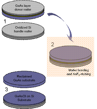
a) 衬底制备工艺
Schematic of GaAsOI fabrication process
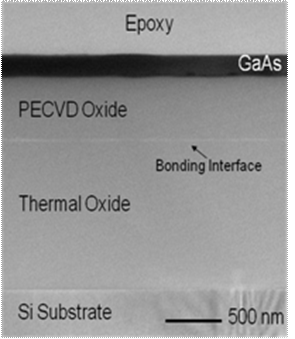
b) GaAsOI/Si 结构透射电镜图片
XTEM image demonstrating a high quality GaAsOI/Si structure obtained with our low temperature bonding and gas-phase ELO procedure.
详见论文/For details see the following paper:
Y. Bai, G. D. Cole , M.T. Bulsara and E. A. Fitzgerald, Sacrificial Etching of Ge by Xenon Difluoride (XeF2) for Fabrication of GaAs-on-Insulator (GaAsOI), Journal of electrochemical society, Volume 159, Issue 2, pp. H183-H190 (2012)
|
|
|